Due Thursday, July 31, 2014 @ 23:59:59
Goals
This assignment will check your understanding of Moore's Law, synchronous digital systems, state elements, combinational logic, and CPU control and datapath.
Submission
Submit your solution by creating a directory named hw5 that contains hw5.txt and hw5fsm.circ.
(File names are case-sensitive and the submission program will not
accept your submission if your file names differ at all from those
specified) From within that directory, type submit hw5. Partners are not allowed on this assignment.
Copy the contents of ~cs61c/hw/05 to a suitable location in your home directory to obtain files you will want for this homework.
$ cp -r ~cs61c/hw/05 ~/hw5
Exercises
Problem 1: Pipelining
Suppose we had the following "silly accumulator." It makes use of an XOR'er, an adder, and a subtracter.
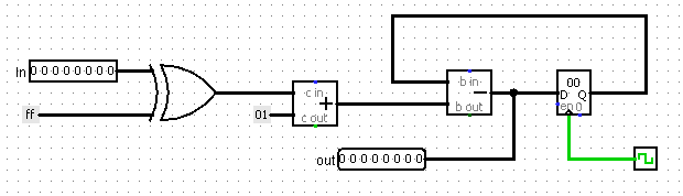
Component specs:
- propogation delay of XOR'er = 20 ns
- propogation delay of adder = 30 ns
- propogation delay of subtracter = 30 ns
- clk-to-q delay of a register = 25 ns
- negligible register setup and hold times (~0 ns)
Assume that the input comes from a clocked register (i.e. its value updates a clk-to-q delay after a clock trigger).
- Calculate the maximum clock rate at which this circuit can operate before pipelining.
- Calculate the maximum clock rate for the three-stage pipelined version of the circuit.
- What is the delay for the output to change in the non-pipelined version? What about the pipelined version?
- What is the least number of inputs that must be given to the circuit in order to finish accumulating faster with the pipelined version?
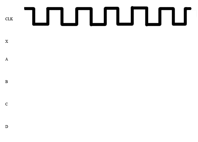
Problem 2: Waveform Diagrams
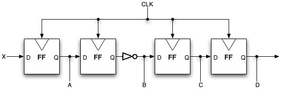
Consider the circuit of Flip-Flops (FF) shown here. Assume that input X alternates between 1 and 0, 10ns after every rising edge. Initially, X is 0 (so 10ns after the first rising edge it should be 1) while A, B, C, and D are unknown. Assume one clock cycle is 30 ns. Given the clock signal, draw the wave for input X, and the signals at points A, B, C, and D in the circuit for the first 6 clock cycles. Assume that the clk-to-q delay is 5 ns, the setup time is negligible (~0 ns), and the hold time is 5ns. Assume that Flip-Flops take their new value on the rising edge of the clock cycle. Assume time = 0 on the first rising edge. Note the NOT gate that precedes B (you may ignore propagation delay for this problem).
Answer the following questions. You would want to fill out the waveform diagram below to help though you don't have to submit it. Consider six clock cycles (so six rising edges) as shown in the diagram. Assume the diagram is cut off 5ns after the last rising edge. You only need to consider from t = 0 ns to t = 155 ns for this problem.
 |
|
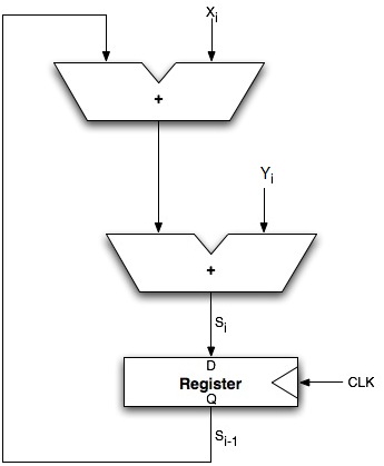
Problem 3: Clock Frequency
Consider this circuit. It accumulates two arguments at a time, arriving at each clock period. You are given the following: the adder propagation delay is 1 ns, the register setup time is 2 ns, the register hold time is 2 ns, the register clk-to-q delay is 3 ns, and the clock frequency is 100 MHz.
 |
|
Problem 4: Simple FSM and Truth Tables
Design an FSM that would take an infinite stream of bits and output 1 twice if it sees two consecutive 1's. In other words, given some input Xi, if Xi-2 = Xi-1 = 1 or Xi-1 = Xi = 1, then it will output 1. Then convert it into a truth table mapping each state and input to a next state and an output. Name the states meaningfully so that it is easily understandable (for example, Seen1 and Seen11). You should have at most four states only. You only need to submit the truth table; you do not need to submit your drawing of the FSM.
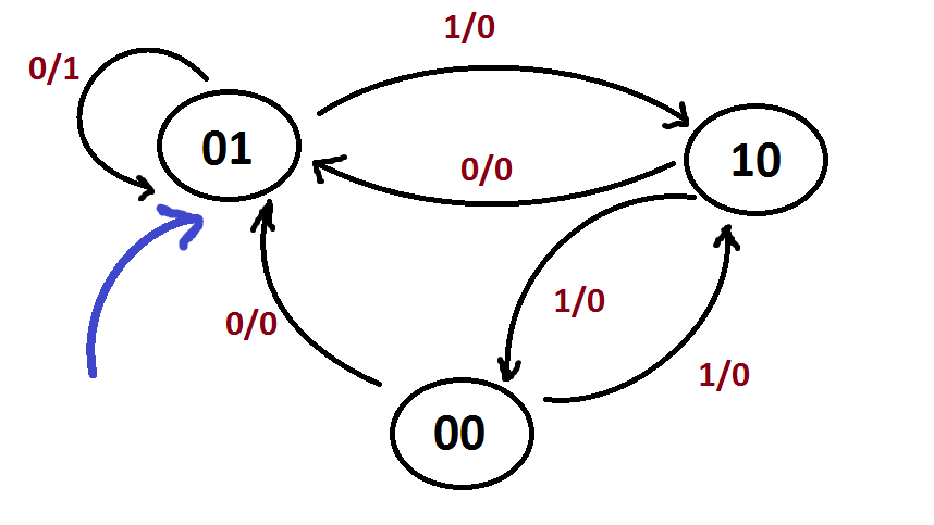
Problem 5: Truth Tables, Boolean Algebra, FSMs, Logic Circuits
Consider the following finite state machine.
|
|
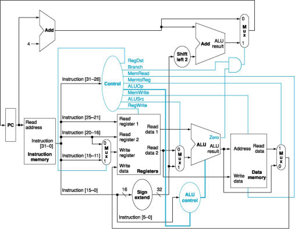
Problem 6: Datapath+Control
Consider the simple single-cycle datapath . The following table describes the control signals for several instructions: (See the textbook or lecture slides for more detailed descriptions of the signals.)
| Instruction | RegDst | ALUSrc | MemToReg | RegWrite | MemRead | MemWrite | Branch |
| addu | 1 | 0 | 0 | 1 | 0 | 0 | 0 |
| lw | 0 | 1 | 1 | 1 | 1 | 0 | 0 |
| sw | X | 1 | X | 0 | 0 | 1 | 0 |
| beq | X | 0 | X | 0 | 0 | 0 | 1 |
Suppose we wish to add the instructions
-
jal(jump and link) and -
ori(or immediate)
- List any necessary datapaths and control signals required for jal and ori to work in the current single-cycle datapath. Be brief for each signal; include from where it comes from, to where it goes, and what it is for. You may add new signals or use existing signals.
- Then expand the table above to include a
jalrow and aorirow as well as additional columns for any control signals that you might have added. - A friend is proposing to modify this single-cycle datapath by eliminating the control signal MemToReg. The multiplexor that has MemtoReg as an input will instead use MemRead. Will your friend's modification work? Explain. What about replacing the MemToReg signal with the MemWrite control signal? For each case, make sure to consider other instructions we've seen (rather than the ones just listed here), and explain what kind of incorrect values will be written and to where if the modification does not work.