Due Wednesday, July 25, 2012 @ 11:59pm
Updates
- July 25, 2012 - Clarification to problem 1. Reworded last problem and problem 3.
- July 23, 2012 - Clarified Problem 1.
- July 22, 2012 - Changed Problem 4 part 2 requirement to make it simpler.
Goals
This assignment will check your understanding of synchronous digital systems, state elements, combinational logic, and CPU control and datapath.
Submission
Submit your solution by creating a directory named hw4 that contains hw4.txt and hw4fsm.circ.
(File names are case-sensitive and the submission program will not
accept your submission if your file names differ at all from those
specified) From within that directory, type submit hw4. Partners are not allowed on this assignment.
Copy the contents of ~cs61c/hw/4 to a suitable location in your home directory to obtain files you will want for this homework.
$ cp -r ~cs61c/hw/04/ ~/hw4
Exercises
Problem 1: Waveform Diagrams - 2 pts
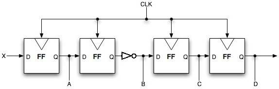
Consider the circuit of Flip-Flops (FF) shown here. Assume that input X alternates between 1 and 0, 25ns after every rising edge. Initially, X is 0 (so 25ns after the first rising edge it should be 1) while A, B, C, and D are unknown. Assume one clock cycle is 75 ns. Given the clock signal, draw the wave for input X, and the signals at points A, B, C, and D in the circuit for the first 6 clock cycles. Assume that the clk-to-q delay is 10 ns and a hold time of 5ns. Assume that Flip-Flops take their new value on the rising edge of the clock cycle. Assume time = 0 on the first rising edge. Note the NOT gate that precedes B (you may ignore propagation delay for this problem).
Answer the following questions. You would want to fill out the waveform diagram below to help though you don't have to submit it.
Consider six clock cycles (so six rising edges) as shown in the diagram. Assume the diagram is cut off 5ns after the last rising edge.
 |
|
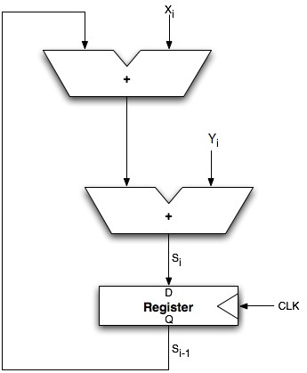
Problem 2: Clock Frequency - 2 pts
Consider this circuit. It accumulates two arguments at a time. You are given the following: the adder propagation delay is 4 ns, the register setup time is 2 ns, the register clk-to-q delay is 1 ns, and the clock frequency is 50 MHz.
 |
|
Problem 3: Simple FSM and Truth Tables - 2 pts
Design an FSM that would take an infinite stream of bits and output 1 only if it has seen both a 1 and a 0
Problem 4: Truth Tables, Boolean Algebra, FSMs, Logic Circuits - 3 pts
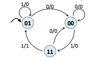
Consider the following finite state machine.
|
|
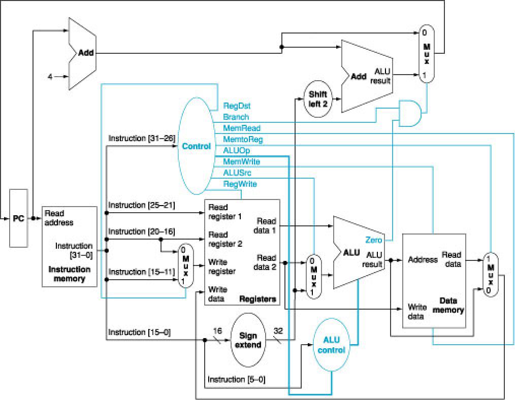
Problem 5: Datapath+Control - 3 pts
Consider the simple single-cycle datapath . The following table describes the control signals for several instructions: (See the textbook or lecture slides for more detailed descriptions of the signals.)
| Instruction | RegDst | ALUSrc | MemToReg | RegWrite | MemRead | MemWrite | Branch |
| addu | 1 | 0 | 0 | 1 | 0 | 0 | 0 |
| lw | 0 | 1 | 1 | 1 | 1 | 0 | 0 |
| sw | X | 1 | X | 0 | 0 | 1 | 0 |
| beq | X | 0 | X | 0 | 0 | 0 | 1 |
Suppose we wish to add the instructions
-
jr(jump register) and -
sll(shift left logical)
- List any necessary
additional signals and muxes in the current single-cycle datapath. Be brief for each signal; include from where it comes from, to where it goes, and what it is for. - Then expand the table above to include a
jrrow and asllrow as well as additional columns for any control signals that you might have added. - A friend is proposing to modify this single-cycle datapath by eliminating the control signal MemToReg. The multiplexor that has MemtoReg as an input will instead use ALUSrc. Will your friend's modification work? What about replacing the MemToReg signal with the MemRead control signal? Explain. Make sure to consider other instructions we've seen (rather than the ones just listed here).