|
In Lab 4, you will design a memory system for your pipelined processor. We will give you a large part of the memory system: a DRAM controller with an integrated instruction cache. The block we supply will have two processor-facing ports: an instruction port and a data port. Your major tasks in this lab will be to (1) design a data cache that works with the data port, and (2) integrate the complete memory system into your Lab 3 design. You will create a test plan for your processor + memory system, and use the test plan to confirm that your processor correctly executes instructions with the memory system.
Lab 4 has several "checkoffs" and a final deadline:
Lab Report Submission Policies: To submit your lab report, run m:\bin\submit-fall2004.exe, or at command prompt type "submit-fall2004.exe" then follow the instructions. The required format for lab reports is shown on the resources page, as is the required format for your design notebook.
Lab 4 Document History:
Before your group begins the design, you will perform several preparatory tasks.
Your group will prepare a design document. The design document will be 2-4 pages in length, and will contain:
See the start of this document for the deadlines associated with the design document (preliminary submission, TA review, and final submission). You are encouraged to submit the preliminary document early, to speed the TA review process.
To help us understand how your team is functioning we require you to evaluate yourself and each of your team members individually.
To evaluate yourself, give us a list of the portions of Lab 3 that you were originally assigned to work on, as well as the set of things that you eventually ended up doing (these are not necessarily the same, and we realize this).
Next, based on your own observations, evaluate the performance of the other members of your team during the last lab assignment. Do not evaluate yourself. Assume an average team member would receive a score of 20 points. Top performers would receive more points, poor performers would receive fewer points.
The maximum score for a person is 40 points. Each evaluation should have a one or two sentence justification for the evaluation. See the Lab 2 writeup for an example evaluation.
You should reevaluate your team members after every lab assignment and base your evaluation only on their performance during that lab assignment. These scores will be used for grading. Be honest and fair as you would hope others will be.
See the schedule at the front of the lab for the due date for the evaluations. Note that each team member emails a separate evaluation report.
As part of this lab, your group will keep an on-line notebook. See the Lab 2 writeup for detailed information about the notebook.
In this section, we describe the memory system IP (IP stands for Intellectual Property -- industry jargon for large pre-made blocks) we have created for you to use in your project. The IP is written in Verilog, and contains a DRAM controller and an instruction cache.
The code and documentation files for this lab are located in m:\lab4. The directory contains a new TopLevel.v file. The directory also contains a DRAM simulator (mt48lc8m16a2.v) so that you can test your memory system without going to the board.
The IP does not include DRAM. Instead, you connect the IP DRAM port to the Xilinx pins that connect to the Calinx DRAM (when going to the board) or to the DRAM simulator (to use ModelSim).
In addition to the DRAM port, the IP contains two independent processor-facing ports: the I port and the M port. The I port provides access to the instruction cache (the IP fills this cache from the DRAM on a miss). The M port provides access to DRAM memory.
Note that the IP time-shares access to the DRAM across several sources: M port accesses, instruction cache misses, and DRAM refresh. We call this time-sharing arbitration.
On the M port, your processor sees the impact of arbitration via the data_ready signal. If you request data on the M port, but the IP is busy doing a DRAM refresh, the IP will signal this busy condition by keeping the data_ready line low until refresh is complete.
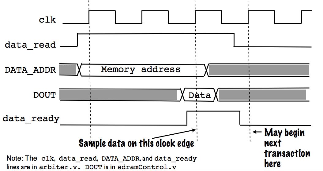
The M port interface is distributed across the arbiter.v and sdramControl.v files (see the "Note" in Figures 1 and 2 for details). Below, we show the bus signals for the M port:
input data_read;        // processor sets it to 1 to make a read request
input data_write;       // processor sets it to 1 to make a write request

input DATA_ADDR[31:0];  // processor puts read address on these lines
input DATA_WRITE_ADDR[31:0];  // processor puts write address on these lines

input DIN[31:0];        // input data
output DOUT[31:0];      // output data

output data_ready;      // signals data has been read or written
The port also defines a clock input, to be driven by the processor clock, and a reset signal.
We now describe M port transaction semantics. We assume the data_ready signal is low. To start a read, the processor asserts the "data_read" line before a rising clock edge. On this edge, the processor also ensures the "DATA_ADDR" lines are stable with the read address. On subsequent rising clock edges, the processor samples the data_ready line. If data_ready is high, the data is present on the DOUT line. The data_ready signal is guaranteed to return to zero for the next rising clock edge, on which the processor may initiate a new transaction. The figure below shows a read transaction.
|
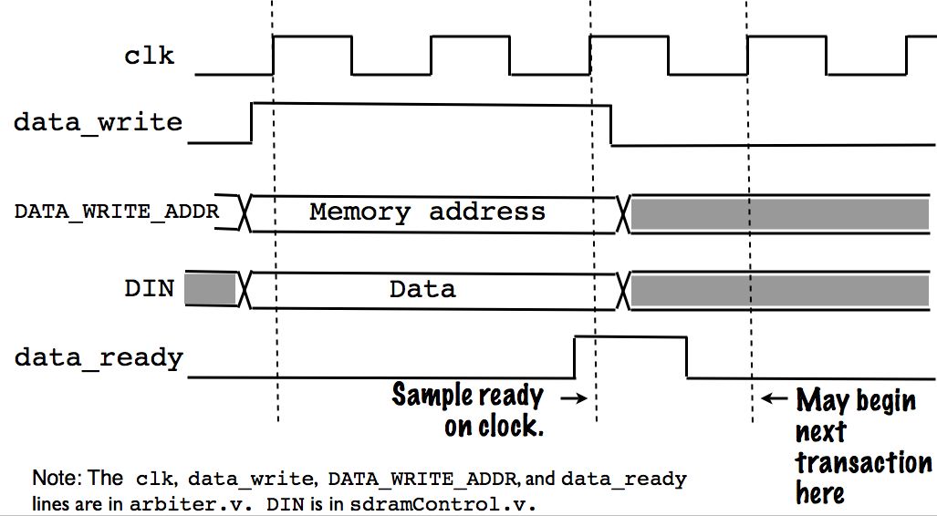
A write transaction is similar. To start a write, the processor asserts the "data_write" line on a rising clock edge. On this edge, the processor also ensures the "DATA_WRITE_ADDR" and "DIN lines are stable with the read address. The processor must keep the data_write line high on subsequent rising clock edges, until the data_ready signal is high on a rising clock edge. The data_ready signal will return to zero for the next clock edge, on which the processor may initiate a new transaction. The figure below shows a write transaction.
|
Like the M port, the instruction cache I port has variable latency -- if a cache miss occurs, the port may take many cycles to return the next instruction. See the documentation in M:\lab4 for a description of the I port, including timing diagrams.
The next step is to design your data cache. The cache you design must have the following properties:
You may choose any block size for the cache you wish (truly an option: no "extra credit" points for choosing a block size that is harder to implement). Recommended options are a 1 word block size (for easy interface to the memory port) or a 4 word block size.
If you choose to implement a 4 word block size, we recommend building a module that converts the M bus interface into a 4 word bus interface, and then design your cache controller to use the wide interface. This approach will simplify reusing your data cache design in the final project.
If you wish, you can use CoreGen to generate your own custom RAM components. Feel free to use any feature of CoreGen you wish (dual-porting, FIFOs, etc).
You may also generate asynchronous RAM blocks. However, you should keep in mind that the asynchronous RAMs are built of LUTs, and that if you attempt to build your entire cache system out of asynchronous RAM you are likely to exhaust all the LUTs on the board.
In addition to designing your data cache, you also need to change the instruction memory interface to your processor, to handle the I bus from the IP. Note that this is tricky because in the case of a cache miss, the I bus may take many cycles to return the data, forcing your processor to stall.
Note that Lab 4 processor builds on Lab 3. Thus, except for the interface change noted above, the processor itself should have the same features as the previous lab. Also, note that your processor does not have to handle self modifying code (except for the level-0 boot). If the processor receives self modifying code its behavior is undefined.
Problem 2a: Tag File
Build the tag file for the cache. Make sure that you can reset all the valid bits to zero after reset. You are allowed to use smaller SRAM components for tags, etc, if you wish (make sure that they compile properly to SRAMs that work with the board).
Problem 2b: Write Buffer
Processor writes to the data cache will go into the cache (if a particular cache line is cached) and will also go directly to DRAM (via the M port on the IP). This can be a serious bottleneck, since it means that every processor write takes a complete DRAM write cycle.
To ameliorate this problem, design a 4-entry write buffer for your system, as we showed in class. This buffer should take writes from the processor and hold them until the M port is ready for a new transaction. Whenever the buffer is full, you must stall the processor from writing.
Each entry will have a 32-bit address, a 32-bit data word, and a valid bit. Make sure to make this 4-entry write buffer fully-associative so that values sitting in the buffer will be returned properly from load instructions.
Processor load instructions should be handled as follows. First, the memory controller should check in the write buffer. If there is an entry there with the right address, the controller should return the value directly from the write buffer. Otherwise, the controller should looks in the cache. If there is a value available, then the controller returns the value immediately. Otherwise, the controller stalls the load and requests a cache fill from the M port.
Processor store instructions should be handled as follows. First, the controller checks the write buffer. If the write buffer contains an entry with the same address as the store instruction, the controller overwrites the entry. Otherwise, if there is a free write buffer entry, the controller uses it for the store. Otherwise, the controller stalls the store until an entry is free.
The M port will see two types of transactions from the data cache. Either (1) it will see read(s) during a cache miss, or (2) it will see a single word write. Note that when we decide to empty a single-word write from the write buffer, we will write it to the M port, and also write it to the cache if the word is properly cached.
The write buffer should be emptied in FIFO order (oldest write
first).
Problem 2c: Pipeline Stalling
Mechanism
Carefully think through how data cache misses will stall the memory stage of your pipeline. Also carefully think through how an instruction cache miss will stall the fetch stage of your pipeline.
For pipeline stalls, be sure to "freeze up and bubble down". Thus, for instance, if you get a cache miss on a load in the memory stage, you should stall this load by (1) freezing the Fetch, Decode, Execute, and Memory stages (i.e. these stages don't move forward and keep repeating the same operations over and over), and (2) send a bubble on to the write stage. This will keep the load instruction in the memory stage. You should then keep stalling until the cache is filled and then release the pipeline to move forward; in the cycle that you release things, the load will be retried and continue as if nothing happened. Stores will stall if the write buffer is full; same thing -- the store keeps retrying until it is able to write into the write buffer.
The important idea here is that requests are submitted to the cache at the beginning of the cycle. Optionally (by the end of the cycle), the cache can reject a request and continue rejecting this request on subsequent cycles until it is ready to satisfy the request. If you do this correctly, you can allow the cache to stall for an arbitrary time.
Come up with a complete mechanism for handling stalls generated by your data cache and by the I bus. Explain your mechanism, and provide timing diagrams.
Problem 2d: Testing
Make a test bench to do multi-unit testing on your data cache (i.e. cache disconnected from the processor, and at your discretion, also disconnected from the IP). Systematically create a test vector suite to verify cache functionality. The more thoroughly you test the data cache here, the easier processor assembly will be! You must be careful to keep the testing readable and concise for grading. Remember, we don't like looking at waveforms in the lab report.
We have several enhancements that you must make to the I/O module. We will be adding to the address space we used in Lab 3. There are 4 distinct address ranges to handle.
Problem 3a: Miscellaneous I/O
In the previous lab, we set I/O space in the
top-4
words. Now, we are using some of the areas that were "Reserved for
future use".
|
|
|
|
| 0x80000000-0x80002000 |
See 4c |
See 4c |
| 0x80002004-0xFFFFFEDC |
Reserved
for future use |
Reserved
for future use |
| 0xFFFFFEE0-0xFFFFFEE8 |
See 4d |
See 4d |
| 0xFFFFFEEC-0xFFFFFEFC | Reserved
for future use |
Reserved
for future use |
| 0xFFFFFF00-0xFFFFFFEC |
See 4b |
See 4b |
| 0xFFFFFFF0 | DP0 | DPO |
| 0xFFFFFFF4 | DP1 | DP1 |
| 0xFFFFFFF8 | Input switches | Nothing |
| 0xFFFFFFFC | Cycle Counter | Nothing |
As in Lab 3, DP0 and DP1 are the registers whose outputs appear on the HEX LEDs. The new entity is the cycle counter. This is a 32-bit counter that counts once per cycle. It will be used to measure statistics. Notice that it should be reset to zero on processor RESET and just count from that point on.
Problem 3b: Level 0 Boot
The I port interface includes a 28-word ROM that appears from Address 0xFFFFFF00 - 0xFFFFFF6C. Note that this work is done for you -- you do not have to create the ROM yourself.
Instruction reads from this address range will return the
corresponding instruction. All data memory accesses to this range will
have undefined results. To use this ROM to boot, arrange your RESET
sequence so that the first PC is always 0xFFFFFF00.
|
|
|
| 0xFFFFFF00 | lui $8, 0x4849 #Initial Display |
| 0xFFFFFF04 | ori $8, $8, 0x2045 |
| 0xFFFFFF08 |
sw $8, -288($0) |
| 0xFFFFFF0C |
lui $8, 0x4152 |
| 0xFFFFFF10 | ori $8, $8, 0x5448 |
| 0xFFFFFF14 | sw $8, -284($0) |
| 0xFFFFFF18 | sw $8, -16($0) #Put "DEADBEEF" on display |
| 0xFFFFFF1C | lui $1, 0x8000 #Instruction I/O Space |
| 0xFFFFFF20 | ori $7, $1, 0x2000 #Limit of 8K |
| 0xFFFFFF24 | j L3 #Go copy first block |
| 0xFFFFFF28 | lw $8, 4($1) #Save instruction address |
| 0xFFFFFF2C | L1: addiu $1, $1, 8 #Skip block header |
| 0xFFFFFF30 | L2: lw $4, 0($1) #Next word |
| 0xFFFFFF34 | sw $4, 0($2) #Copy to memory |
| 0xFFFFFF38 | addiu $3, $3, -1 #Decrement count |
| 0xFFFFFF3C | addiu $1, $1, 4 #Increment source |
| 0xFFFFFF40 | bne $3, $0, L2 #Not done |
| 0xFFFFFF44 | addiu $2, $2, 4 #Increment destination |
| 0xFFFFFF48 | sltu $5, $1, $7 #Run over limit? |
| 0xFFFFFF4C | beq $5, $0, BADEND #Yes. Format problem? |
| 0xFFFFFF50 | L3: lw $3, 0($1) #Get next length |
| 0xFFFFFF54 | bne $3, $0, L1 #Non-zero? Yes, copy |
| 0xFFFFFF58 | lw $2, 4($1) #Get next address |
| 0xFFFFFF5C | END:sw $8, -16($0) #Put execution addr in DP0 |
| 0xFFFFFF60 | jr $8 #Start Executing |
| 0xFFFFFF64 | break 0xAA #Pause with 10101010 |
| 0xFFFFFF68 | BADEND: j BADEND #Loop forever |
| 0xFFFFFF6C | break 0x7F #Indicate problem! |
You can modify the level 0 boot ROM any way you like, but it must fit within the following address range 0xFFFFFF00-0xFFFFFFEC and it must incorporate the basic functionality laid out above. Notice that what happens here is that the code looks for a compact description of instructions starting at address 0x80000000. The format of the block of memory at that address is:
Block 0: Length0
Address0
Block0[0]
Block0[1]
...
Block0[Length0-1]
Block 1: Length1
Address1
Block1[0]
Block1[1]
...
Block1[Length1-1]
Block 2: Length2
...
This sequence is terminated with a zero Length field. It is assumed that Block 0 is a block of instructions and that the system should start executing at Address0 after it is finished copying data. The idea here is that you can have a sequence of instructions that is copied one place in memory and a sequence of data that is copied elsewhere.
Problem 3c: Data Source
You should use either the TFTP Blackbox (highly
recommended) or one of the synchronous RAM blocks (only if the black
box doesn't work) from Lab 3 for your data source. Assume that you
produce data in
the above format. Compile it into a 2Kx32 block, then download it to
your board. Reads from addresses 0x80000000
- 0x80001FFC should read
from this
block. To reproduce what we had in Lab 3, you will simply add a length
header
and an address of 0x00000000 to the front of your instructions output
from MIPSASM and a word of 0x00000000 to the end of the output. You may
find some of MIPSASM's more advanced features useful in specifying
higher address ranges and automatically calculating the length of the
code.
For example here is a code sample that will generate the proper header and footer for a simple code block:
.count
words begin end # Count the number of words between the begin and end
labels
.word 0x00000000 #
Place the starting address
.address 0x00000000 # Direct
MIPSASM to use 0x00000000 as the address when performing jumps
begin:
srl $0, $0, 0
srl $0, $0, 0
srl $0, $0, 0
srl $0, $0, 0
srl $0, $0, 0
end:
.word 0x00000000 # A trailing
0x00000000 terminates the instruction stream
Something more fancy might be:
.count
words begin1 end1 # Count the number of words in the instruction segment
.word 0x00000000 #
Instruction segment starting address
.address 0x00000000 # Direct
MIPSASM to use 0x00000000 as the address when performing jumps
begin1:
srl $0, $0, 0
srl $0, $0, 0
srl $0, $0, 0
srl $0, $0, 0
srl $0, $0, 0
end1:
.count words begin2 end2 # Count the number of words in the data segment
.word 0x00100000 # Data
segment starting address
.address 0x00100000 # Direct MIPSASM to use 0x00100000 as
the address when performing jumps
begin2:
.word 0x00000001
.word 0x00000002
.word 0x00000003
Note that writes to this address range are
undefined.
Problem 3d: ASCII Text Conversion
The TAs have provided an ASCII conversion tool that takes an ASCII code
in 7 bits and outputs 7 bits of coding information for the hexadecimal
LEDs. Note that not all characters can be displayed on the LEDs,
so some characters will be converted to a black space.
ASCII_REG1 is a 28 bit register that contains
the
ASCII-converted display information for hexadecimal LEDs 1-4.
ASCII_REG2 is a 28 bit register that
contains the ASCII-converted display information for hexadecimal LEDs
5-8.
POINT_REG is an 8 bit register that contains the display information
for the LED decimal point segments. The high bit corresponds to
LED point 1. A high value indicates that the LED point is turned
on.
|
|
|
|
| 0xFFFFFEE0 | Nothing |
Convert the stored value into
ASCII and store it in ASCII_REG1. |
| 0xFFFFFEE4 | Nothing | Convert the stored value into ASCII and store it in ASCII_REG2. |
| 0xFFFFFEE8 | Nothing |
Store the low 8 bits of the word into POINT_REG. Bit 7 corresponds to the high bit of POINT_REG and bit 0 corresponds to the low bit of point reg. Ignore the high 24 bits. |
Finally, tie your lab together. You should have all of the I/O from your previous lab. Further, you should make a new file called "boardlevel.v" that includes (1) the new TopLevel.v from the high-level directory and (2) a simulation of the DRAM banks as they appear on the board.
Just as in Lab 3, you should do complete processor testing of your processor. Produce an extensive test suite to make sure that everything still works. You should use the same test programs from last lab plus a bunch of new ones.
After verifying your complete design works in simulation, push the design to the board, and run it on real hardware.
Your lab report should contain a description of (a) how the I bus interface to your process operates (b) how your data cache operates (c) how you handle pipeline stalls. Also, tell us the size of your processor: how many slices did you use/what fraction of the Xilinx chip did you use?
Determine the critical path of your processor. Document (using data from the Xilinx timing tools) why you believe the critical path is what you claim. How did you determine your component delay values?
Next, measure the running speed of your processor. What is the fastest clock that you think you can run with? Can your memory subsystem run at the same speed as your processor clock? How does this measurement square with your critical path determination?
Turn in a copy of your Verilog code (including test benches), schematics, diagnostic program(s) and your on-line logs. Also turn in simulation logs that show correct operation of the processor + memory system. These logs should show the operations that were performed, and then the contents of memory with the correct values in it. Also turn in logs from your test benches.
As part of your writeup, do a port-mortem for your test plan. How did unit testing, multi-unit testing, and complete processor testing help your verification and debugging? Show bug curves, and give examples of the type of bugs you found early on because of your test plan (as well as "escaped" bugs you found later than you would have hoped).
How much time did your team spend on this assignment?