Lab 0: FPGA Development Board Introduction
0 Before you begin
This lab is intended to both introduce the CS 150 development
platform and take care of administrative tasks. You will need to complete the following
steps before you can begin working on the lab (and these are considered requirements
for completion of the lab):
- Pick up a cs150-xx class account during your scheduled lab section.
- Log into one of the CentOS lab machines (p380-{11..45}.eecs). On your first time logging in you will need to select a session (GNOME or KDE) or it will fail.
- Open a terminal and run passwd to set your password.
- Register your account for the course so you appear in glookup. In the terminal:
- SSH into cory (glookup/register only
work on Solaris machines):
ssh cory - Run register, enter your information, then exit the ssh connection
- Make sure you have access to the CS 150 Piazza forum; if not, signup here.
- Read the Course Lab Guide
- Make sure you have card key access to 125 Cory. If not, follow these instructions.
- Read through and understand this document before you start working!
1 Development Platform
CS 150 uses the XUPV5-LX110T development board, located on the lab bench next to your workstation. The following image identifies important parts of the board:
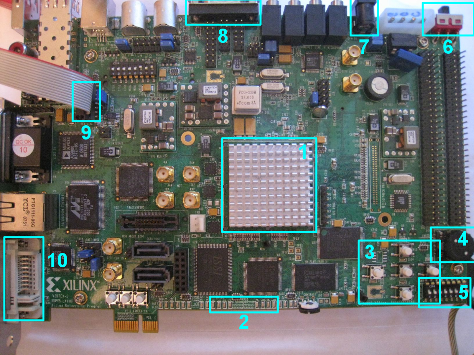
- Virtex-5 FPGA (covered by heat sink)
- GPIO LEDs, numbered 0-7
- NESW & center buttons, each with a corresponding LED
- Rotary encoder
- GPIO DIP swtiches, numbered 1-8 (but 0-7 in code).
- Board power switch
- Power connector
- Serial port
- JTAG header
- DVI-I connector
2 Structural Verilog Introduction
Note: This lab assumes you have basic familiarity with logic gates and Boolean algebra. Consult this document if you need to review either topic.
Throughout the semester, you will build increasingly complex designs using Verilog, a widely used hardware description language (HDL). For this lab, you will learn structural Verilog, a limited subset of Verilog that allows you to describe circuits in terms of wires, gates and modules.
2.1 Wires
Wires in structural Verilog are analogous to wires in a circuit you build by hand: they are used to transmit values between inputs and outputs.
Wires should be declared before they are used:
wire a;
wire b, c; // declare multiple wires using commas
The wires above are scalar (i.e. represent 1 bit). They can also be vectors:
wire [7:0] d; // 8-bit wire declaration
wire [31:0] e; // 32-bit wire declaration
Wires can be assigned to other wires, concatenated, and indexed:
wire [31:0] f;
assign f = {d, e[23:0]}; // concatenate d with bottom 24 bits of e
In the line above, the brackets [] are used to index a 24-bit range of e and the braces {} concatenate comma-separated wires.
2.2 Gates (Structural Primitives)
In this lab, you may use the following primitives: and, or, xor, not, nand, nor, xnor. In general, the syntax is:
operator (output, input1, input2);
For example, the following Verilog implements the Boolean equation F = a + b:
wire a, b, F;
/* … some code that assigns values to a and b */
or (F, a, b);
Complex logic functions can be implemented using intermediate wires between these primitive gates.
2.3 Modules
Modules provide a means of abstraction and encapsulation for your design. They consist of a port declaration and Verilog code to implement the desired functionality. For example, consider a module that computes y = (a + b)(c + d):
module example_module(a, b, c, d, y);
// Port and wire declarations:
input wire a, b, c, d;
output wire y;
wire a_or_b, c_or_d;
// Logic:
or (a_or_b, a, b);
or (c_or_d, c, d);
and (y, a_or_b, c_or_d);
endmodule
There are a few things to note from this example:
- The ports must be declared as input or output wires, but can be thought of as wires within the module.
- Wires declared within a module (such as a_or_b) are limited in scope to that module.
- Modules should be created in a Verilog file (.v) where the filename matches the module name (so the above example should be located in example_module.v).
Then, after creating a module, you can instantiate it in other modules:
example_module unique_name(
.a(a),
.b(b),
.c(c),
.d(d),
.y(result));
(Assuming a, b, c, d, and result are valid wires in the module that this instantiation occurs in,
and unique_name is globally unique)
The syntax .<input/output>(<wire>) is used to explicitly hook up wires to the correct input/outputs of a module. You can also write
example_module unique_name(a, b, c, d, result); // correct order
which, while perfectly valid, is not recommended since it is possible to mix up the order of the wires. The first form is also easier to read.
example_module unique_name(result, a, b, c, d); // wrong order!
3 Lab Procedure
Follow these steps and make sure to save your work for checkoff as you progress. If you run into any problems during the lab (e.g. design doesn’t work on the board, compiler errors) please ask a TA to look at your code.
3.1 Acquire the lab files
Paste the following commands into your terminal:
cd
mkdir labs
cd labs
curl http://inst.eecs.berkeley.edu/~cs150/sp12/lab0/lab0.tar.gz | tar -xzv
3.2 Existing Functionality
From the src directory, open ml505top.v in your favorite text editor. This is the “top-level” module, which essentially means the input and output ports represent physical connections on the board. The port definition for this module contains an 8-bit input for the GPIO DIP switches (#5 in the diagram) and an 8-bit output to the GPIO LEDs (#2 in the diagram).
The skeleton files provided contain a simple example of an AND gate. This gate takes as inputs GPIO DIP switches 1 and 2, and displays the AND of these on LED 0.
Before you implement the rest of the lab, verify this functionality in hardware:
- Run ‘make’ in the lab0 directory. This performs several steps to interpret your code and generate a configuration bitstream for the board. You will learn about these steps over the next few labs.
- Verify that the LED on the Xilinx Platform Cable (picture) is glowing green. If it isn’t, verify that the FPGA is powered on and that there a USB cable connected between the Xilinx Platform Cable and the computer.
- After make completes, run ‘make impact’ from the same directory. This programs the FPGA with the bitstream file created in step 1.
- The design should now be on the board. Verify that LED 0 displays the AND of GPIO switches 1 and 2.
3.3 2-1 Mux
You should also see an instantiation of Mux2_1 in ml505top.v. Implement this module in Mux2_1.v (so that it conforms to the functionality in the file’s comments) and follow the steps in section 3.2 to test this on hardware.
3.4 Full Adder
Next, examine the port definition of FA.v. Following the instruction’s in the comments of ml505top.v, write the instantiation of FA in the top file. You may find it helpful to look at the instantiation of Mux2_1 as an example.
Finally, using only structural Verilog, implement a full adder circuit in FA.v. If you are not familiar with the functionality of a full adder, the truth table and one possible gate diagram is shown below:

|
A |
B |
Cin |
Sum |
Cout |
|
|
0 |
0 |
0 |
0 |
0 |
|
|
0 |
0 |
1 |
1 |
0 |
|
|
0 |
1 |
0 |
1 |
0 |
|
|
0 |
1 |
1 |
0 |
1 |
|
|
1 |
0 |
0 |
1 |
0 |
|
|
1 |
0 |
1 |
0 |
1 |
|
|
1 |
1 |
0 |
0 |
1 |
|
|
1 |
1 |
1 |
1 |
1 |
Again, you should be able to follow the steps in section 3.2 to test the adder on hardware.
4 Checkoff
For checkoff, you will show a TA your implementation on hardware as well as your answers to the checkoff questions. Please have them open in a text editor or written on paper (they are not collected so there is no need to print if you type).
Checkoff for this lab is due before the end of your lab section. For the remainder of the labs, checkoffs will be due at the beginning of the following week’s lab section.
To be checked off for Lab 0:
- Show the adder and mux working on the board.
- Show the 3 Verilog files you modified.
- How many logic gates did your adder require?’