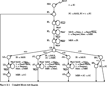
Figure 12.1 gives the complete state diagram, including register transfer
operations, for a Moore machine implementation of the processor of Section
11.3. It requires more states than the equivalent Mealy diagram, but the
difference is small. In particular, we need an extra state in the reset/instruction
fetch sequence and another one in the branch negative sequence.
The assignment of register transfer operations to states
is reasonably straightforward. Only one combination of register transfer
operations in the same state is surprising. This is where the memory read
request is used at the same time as latching the memory databus into the
MBR (see states IF2, LD1, and AD1). Does this
result in latching invalid data?
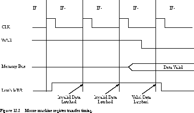
Figure 12.2 shows the detailed timing of events for the state sequence
IF1, IF2, and IF3. Each time we loop in such a state, the MBR captures the
current value of the memory bus. For the first few times looping in the
state, the data captured by the MBR is invalid. However, the Wait signal
remains asserted until the memory places valid data on the bus. When Wait
is unasserted, the value latched into MBR at the next clock transition is
valid. This is the same state transition that advances the state machine
to its next state (IF3, LD2, or AD2).
Moore Machine Block Diagram The block diagram of the Moore machine is given in Figure 12.3.
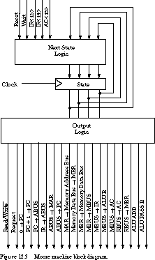
It requires 16 states. We encode this densely in a 4-bit state register.
The next-state logic has nine inputs (four current-state bits, Reset, Wait,
two IR bits, and one AC bit) and four outputs (the next state).
Since the data-path control signals are decoded from the state, this block
of logic has four inputs and 18 outputs.
Implementation Choices: ROM Versus PAL/PLA We
can implement the next-state logic block and the output logic block as either
ROMs or PAL/PLAs. Using ROMs, we can implement the next-state logic by a
512 by 4-bit memory and the output logic by a 16 by 18-bit memory. Since
single device ROMs come in widths that are powers of 2, we would implement
the latter with several 4-bit- or 8-bit-wide ROMs.
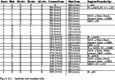
We begin implementing the controller by obtaining the
symbolic next-state table. This is shown in Figure 12.4. A couple of things
are worth observing about this table. First, we can make extensive use of
the don't cares among the inputs/address lines. Notice that a given input
signal is examined in very few states. For example, the IR bits are examined
in state OD and the AC sign bit is tested only in state BR0.
Second, the number of register transfer operations asserted
in any given state is rather small. In Figure 12.4, no more than four register
transfer operations are asserted in any state. Some of the outputs, like
those associated with memory references, are always asserted together. We
will exploit this in some of the controller implementation strategies later
in this chapter.
Of course, a ROM-based implementation cannot take advantage
of don't cares. You must program all 512 ROM words for the next-state logic,
a rather tedious task. However, one advantage of using a ROM is that you
need not worry about a careful state assignment.
If you use a PAL or a PLA, then a good state assignment
is essential for reducing the complexity of the next-state logic. For example,
the naive state assignment suggested by Figure 12.4 (basically,
a depth-first enumeration) yields a 21-product-term implementation.
This compares rather unfavorably with the equivalent of 512 product terms
in the ROM case (one term for each ROM word).
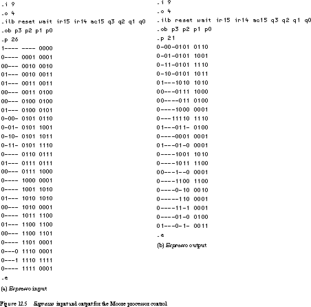
Figure 12.5 shows the espresso inputs and outputs for this particular state assignment. The next-state logic is fairly complex. Each next-state bit requires seven to nine product terms for its implementation. This implies that you should use a PAL component with large OR gate fan-ins, like the P22V10. For a PLA-based implementation, all you need is a PLA that provides 21 unique product terms.
A nova state assignment can do even better. It requires only 18 product terms:
state IF0: 0000  					state ST0: 0101

state IF1: 1011  					state ST1: 0110

state IF2: 1111  					state AD0: 0111

state IF3: 1101  					state AD1: 1000


state  OD:  0001  					state AD2: 1001

state LD0: 0010  	state BR0: 1010

state LD1: 0011  					state BR1: 1100

state LD2: 0100  					state RES: 1110
(four
state outputs and 18 microoperation control outputs).(512 ¥
4 + 16 ¥ 18). The Mealy machine needs 11,264
ROM bits (512 ¥ 22). This shows some of the
inherent inefficiency of the ROM-based approach. Many of those ROM bits
are really don't cares. Of course, ROMs are very dense and even large ROMs
are not too expensive. We will see more efficient methods for using ROMs
in our discussion of microprogramming.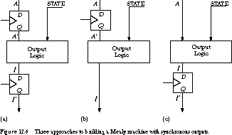
Figure 12.6 shows three possible ways to construct a Mealy machine with
synchronized outputs: using edge-triggered devices (a)
at the input and output, (b) only at the inputs,
and (c) only at the outputs. Each affects the
timing of control signals in a slightly different way. In the figure, we
assume that output should be asserted whenever input A is asserted.
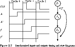
Let's start with case (a),
which synchronizes both the inputs and the outputs. Assuming that A
is asserted in cycle 0, the synchronized output will not be asserted until
cycle 2. This delays the calculation of by two cycles. Thus, if A
is asserted in state S0, the output is not asserted until state
S2. The timing and state diagrams of Figure 12.7 make this more
clear.
You should realize that placing synchronizing registers
at both the inputs and outputs is overkill. We can get the desired synchronization
by placing flip-flops at one side or the other of the output logic. Let's
consider case (b): only the inputs are synchronized.
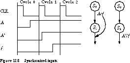
Figure 12.8 shows the effects. If A is asserted in cycle 0, is asserted in the following cycle. Alternatively, we can label the state transitions in the next state with the synchronized input A' and the output .
Case (c) places synchronizing
logic only on the outputs. The timing diagram is similar to Figure 12.8
and is shown in Figure 12.9.
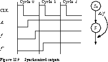
The synchronized output signal ' takes effect in the state after the one in which A is first asserted.
Synchronizing the Simple CPU Mealy State Diagram To
make these ideas concrete, let's examine a Mealy implementation of the processor
control state machine we derived in Section 11.3. Case (b),
which places registers on the inputs, makes the most sense for synchronizing
this machine. Of the five inputs, IR<15:14> and AC<15> are already
synchronized because they are data-path registers clocked by the same clock
as the control state machine. The delayed effect of control signals does
not apply here; we are not placing an additional register in the path between
the IR and the AC and the control. For example, we can load the IR with
a new instruction in one state and compute a multiway branch based on the
op code in the very next state.
Reset and Wait are another matter. Because these signals
come from outside the processor, it is prudent to pass them through synchronizing
flip-flops anyway. This means that the external Reset and Wait signals are
delayed by one clock cycle before they can influence the state machine.
Delaying reset by one cycle has little effect because
the state of the machine will be reset anyway. However, the one state delay
of the Wait signal does affect performance. The processor normally loops
in a state until there is a change in Wait. This means that the machine
stays in the loop for an extra cycle. Even a memory that responds to a request
immediately requires one processor clock cycle before the processor can
recognize that the operation is complete.
If we design the memory system to be synchronous with
the processor, we can avoid this performance loss. Since the memory system's
controller is clocked with the same clock as the processor, the Wait signal
no longer needs to be synchronized.
[Top] [Next]
[Prev]