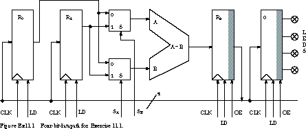
1. (Register Transfer and State Diagrams) Assume
that you have a bus-connected assembly of a 4-bit subtractor and four registers,
as shown in Figure Ex11.1. All registers are positive edge--triggered, and registers R2
and O have tri-state outputs. All buses are 4 bits wide. You are to perform the following sequence of register transfer
-operations: (1) compute R1-R0,
latching the result into R2, (2) display
the result on the LEDs attached to register O, and (3)
replace R0 with the result.
Tabulate all of the register transfer operations and their
detailed microoperations that are supported by this data-path organization.
Create a timing waveform for the control signals LD (load),
S (select), and OE (output
enable) to implement this sequence in a minimum number of clock
cycles. This diagram should include traces for all of the control signals
in the figure: R0:LD, R1:LD, A:S, B:S,
R2:LD, R2:OE, O:LD, O:OE. Recall that
the state changes on the positive edge of the clock, and don't forget to
incorporate signal propagation delays in your timing waveforms.
Show the state diagram, annotated with control signal assertions and their
corresponding register transfer operations, that corresponds to the timing
waveforms you filled out in part (b).
2. (Memory Interface) A
read-only memory and a microprocessor need to communicate asynchronously.
The processor asserts a signal to indicate READ and sets the ADDRESS signals.
The memory asserts COMPLETE when the data is available on the DATA signals.
Draw two simple state diagrams that indicate the behavior of the processor
and the memory controller for a simple read operation. The READ and COMPLETE
signals should follow the four-cycle handshake protocol. Assume that the
memory controller cycles in an initial state waiting for a memory READ request.
3. (Memory Interface) For
the memory interface and state diagrams in this chapter, we assumed a Princeton
architecture. In this exercise, you will rederive these for a Harvard architecture.
Modify the memory interface of Figure 11.5 for a Harvard
architecture. Provide two separate memory interfaces, one for instructions
and one for data.
What changes are necessary in the state diagram of Figure 11.23 to reimplement
this machine for a Harvard -architecture?
What new register transfer operations are needed to support this alternative
memory interface? Modify Figure 11.24 to reflect these additions.
4. (Instruction Prefetch) In
Exercise 11.3 you modified the memory interface to provide separate instruction
and data memories. Modify the state diagram of Figure 11.23 to allow the
next instruction to be fetched while the current instruction is finishing
its execution. Tabulate the register transfer operations used in each state.
5. (Control State Diagram) The
state diagram derived in Section 11.3.2 assumed a synchronous Mealy implementation.
Rederive the state diagram, but this time assume a Moore machine implementation.
Associate the appropriate register transfer operations with the states you
derive. Also describe for each state the function, such as instruction fetch,
operand fetch, or decode that it is implementing.
6. (Datapath Design) Consider
the following portion of a simple instruction set encoded in 4-bit words.
The machine has a single accumulator (R0),
a rotating shifter (R1), four general-purpose
registers (R0, R1, R2, R3),
four accumulator/shifter oriented instructions (COMP, INC,
RSR, ASR), and two register-register instructions (ADD,
AND). In register transfer-like notation, these instructions
are defined as follows:
(c), but this time for the RSR instruction.
(Datapath Design) Repeat
Exercise 11.6, but this time design the data-path using a single-bus interconnection
scheme.(Datapath Design) Repeat
Exercise 11.6, but this time design a compromise multiple-bus data-path.
Your goal should be to reduce the number of states it takes to implement
the ADD and RSR instructions, short of using the point-to-point scheme.(Control State Machine) The
instruction set fragment of Exercise 11.6 provides no way to load the registers.
We add the following multiple-word instructions to accomplish these functions:
| 1100 Y3Y2Y1Y0 | XFER | R[Y3Y2] :=
R[Y1Y0] |
| 1101 Y7Y6Y5Y4 Y3Y2Y1Y0 | LD | R[0] := MEM[Y7Y6Y5Y4
Y3Y2Y1Y0] |
| 1110 Y7Y6Y5Y4 Y3Y2Y1Y0 | ST | MEM[Y7Y6Y5Y4 Y3Y2Y1Y0]
:= R[0] |
(load) and ST (store)
instructions are encoded in three adjacent words: the first denotes the
instruction, the second and third the memory address (this
machine can address up to 256 four-bit words). For completeness,
the last instruction is BRN, Branch if R0 is Negative: | 1111 Y7Y6Y5Y4 Y3Y2Y1Y0 | BRN | IF R[0]<3> =
1 THEN |
| | | PC := Y7Y6Y5Y4 Y3Y2Y1Y0 |
(PC, IR, possibly others). What new register transfer operations and microoperations are
added by these four instructions? (Datapath Design) How
does the register-to-register transfer operation (XFER)
affect your data-path designs in Exercises 11.6 (point-to-point),
11.7 (single bus), and 11.8 (multiple
buses)?(Datapath Design) Put
together a unified data-path, integrating the control registers (PC,
IR, etc.) from Exercise 11.9 with your data-paths from Exercises
11.6, 11.7, and 11.8. How many processor states (total clock
cycles) does it take to implement the ADD and RSR instructions
in each data-path? Explain how you derived your state/cycle count.(Datapath Design) Consider
the following change to the instruction set description of Exercise 11.6.
The RSR and ASR are eliminated from the instruction set and replaced by
the following two -instructions: | 1010 | CLC | CARRY := 0 |
| 1011 | ADC | R[0] := R[0]
+ CARRY |
| | | CARRY := Carry out from ALU |
(add with carry) instruction.(Processor Datapath and Control) Consider
the instruction format for a 16-bit computer in Figure Ex11.13. The high-order
4 bits specify the operation code. Every instruction contains two operands.
The first operand is always one of the processor's general-purpose registers,
which is specified by the Reg A field in the instruction (the
machine has four general-purpose registers, R0, R1, R2,
and R3). The second operand is always in memory. Its
address is formed by the sum of the contents of a register, indicated by
the Reg B field, and the offset value within the instruc-tion. The machine's
initial data-path is shown in Figure Ex11.13. The ALU implements ADD, SUB,
and so forth.(assume the instruction has already been
fetched and decoded), given the following "macrodefinition"
of the add: ADD Ra, (Rb)offset Ra
:= Ra + Memory[Rb +
Offset]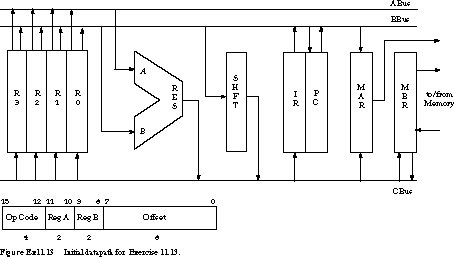 For example, if the instruction
is "Add R0,
For example, if the instruction
is "Add R0, (R1) 10" and R1
contains 5, then the contents of memory location 15 are added to the contents
of R0, with the result stored back into R0.(you may need to add additional paths or operations).
In your answer, show how register transfer operations should be grouped
into states.(assume the instruction has
already been fetched and decoded), given the following macrodefinition
of the branch: BRN Ra, (Rb)offset If
Ra < 0 then PC := Rb + Offset+127 and -128. State any additions to or
assumptions about the data-path that must be made to implement the execution
sequence of this instruction. As in part (b),
group the register transfer instruction into states. (Processor Specification and Datapath
Design) In this exercise, you will describe the architecture
of a simple 4-bit computer. The machine is organized around an evaluation
stack, an ALU that supports the twos complement operations SUB, ADD, and
INCRement and the logical operators AND, OR, and COMPlement, and a rotating
shifter supporting both logical rotating shifts and arithmetic shifts. The
machine supports 16 different instructions, including those for accessing
memory, call/return from subroutine, and conditional/unconditional branches.
These instructions are encoded in one to three 4-bit word parcels. The machine
can address 256 four-bit words, organized as a Harvard architecture.(5
+ 2). This can be implemented by the following
sequence of stack-oriented operations: (a). The expression can be rewritten
without parentheses as 9 5 2 + -. 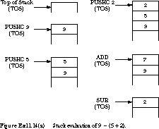
We assume that the Top of Stack pointer is initialized
to -1 at processor restart. This represents an empty stack. The TOS pointer
is incremented before an item is added to the stack, and is decremented
after an item is removed.
Instructions are encoded in one to three four-bit words.
Arithmetic, logical, and shift instructions are encoded in a single word:
all four bits form the op code. The operands are implicitly the elements
on the top of the stack. The arithmetic/logical instructions are: ADD, SUB,
AND, OR, COMP, INCR, RSR (rotating shift to the right),
and ASR (arithmetic shift to the right), and their
encodings are the following:
(Return
from Sub-routine) are encoded in three 4-bit words: one word
for the op code and two words for the target address. The conditional branch
instructions, BRZ and BRN, test the top of stack element for =
0 or < 0, respectively. If true, the PC is changed to the target address.
In either case, the TOS element is left -undisturbed.(Jump to Subroutine) is
a special instruction that is used to implement subroutines. The current
value of the PC is placed on the stack and then the PC is changed to the
-target address. Any values placed on the stack by the subroutine must be
POPed before it returns. The RTS instruction restores the PC from the value
saved on the stack. It is important to organize the processor state machine
so that the PC always points to the next instruction to be fetched while
executing the current -instruction. 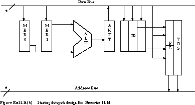
Figure Ex11.14(b) shows an initial data-path
design for this -instruction set.
Extend this data-path with a Harvard architecture memory
-interface.
What register transfer operations and microoperations are supported by this
data-path?
How can the microoperations you found in part (b)
be used to implement the execution portion for each of the 16 instructions
of the instruction set?
15. (Processor Controller Design) Design
a state diagram for the processor and instruction set described in Exercise
11.14. You can choose a Moore or Mealy design style.
Draw the modified state design. Identify in general terms
what is happening in each state.
What microoperations should be associated with each state?
For each of the 16 instructions in the instruction set, describe the number
of states required for its fetch and execution. You may assume that the
memory system responds in a single processor cycle for the purposes of this
calculation.
[Top] [Next] [Prev]