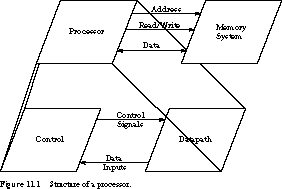
Figure 11.1 shows a high-level block diagram of a computer. It is decomposed
into a central processing unit (CPU), or processor,
and an attached memory system. In turn, the processor is decomposed
into data-path and control units.
The datapath (also called the
execution unit) contains registers for storing intermediate
results and combinational circuits for operating on data, such as shifting,
adding, and multiplying. The latter are sometimes called functional
units because they apply functions to data. Data is moved from memory
into registers. It is then moved to the functional units, where the data
manipulations take place. The results are placed back into registers and
eventually put back into memory. The data-path implements the pathways along
which data can flow from registers to functional units and back again.
The control unit (or instruction
unit) implements a finite state machine that fetches a
stream of instructions from memory. The instructions describe what operations,
such as ADD, should be applied to which operands. The operands can be found
in particular registers or in memory locations.
The control unit interprets or "executes" instructions
by asserting the appropriate signals for manipulating the data-path, at
the right time and in the correct sequence. For example, to add two registers
and place the results in a third register, the control unit (1)
asserts the necessary control signals to move the contents of the two source
registers to the arithmetic logic unit (ALU),
(2) instructs the ALU to perform an ADD operation
by asserting the appropriate signals, and (3)
moves the result to the specified destination register, again by asserting
signals that establish a path between the ALU and the register.
Instructions can be grouped into three broad classes:
data manipulation (add, subtract, etc.), data
staging (load/store data from/to memory), and
control (conditional and unconditional branches).
The latter class determines the next instruction to fetch, sometimes conditionally
based on inputs from the data-path. For example, the instruction may be
to take the branch if the last data-path operation resulted in a negative
number.
You are already familiar with the basic building blocks
needed to implement the processor. You can interconnect NAND and NOR gates
to build adder and logic circuits (Chapter 5)
and registers (Chapters 6 and 7). The processor
control unit is just another finite state machine (Chapters
8, 9, and 10). In the rest of this section, we will examine
the components of a computer in a little more detail, as a prelude to the
rest of this chapter.
Basic States of the Control Unit The control unit can be in one of four basic phases: Reset, Fetch the Next Instruction, Decode the Instruction, and Execute the Instruction. A high-level state diagram for a typical control unit is shown in Figure 11.2.
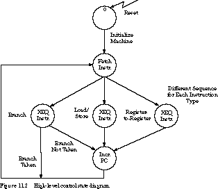
Let's begin with the initialization sequence. An external reset signal places the finite state machine in its initial Reset state, from which the processor is initialized. Since the state of the processor contains more than just the state register of the finite state machine, several of the special registers must also be set to an initial value. For example, the PC must be set to some value, such as 0, before the first instruction can be fetched. Perhaps an accumulator register or a special register holding an indication of the condition of the data-path will be set to 0 as well. Although shown as a single state in the figure, the initialization process may be implemented by a sequence of states.
Next, the machine enters the Fetch Instruction
state. The contents of the PC are sent as an address to the memory system.
Then the control generates the signals needed to commence a memory read.
When the operation is complete, the instruction is available on the memory's
output wires and must be moved into the control unit's IR. Again, Fetch
Instruction looks like a single state in the figure, but the actual implementation
involves a sequence of states.
Once the instruction is available in the IR, the control
examines certain bits within the instruction to determine its type. Each
instruction type leads to a different sequence of execution states. For
example, the basic execution sequence for a register-to-register add instruction
is identical to one for a register-to-register subtract. The operands must
be moved to the ALU and the result directed to the correct register destination.
The only difference is the operation requested of the ALU. As long as the
basic data movements are the same, the control sequences can be parameterized
by the specific operation, decoded directly from the instruction.
The state machine in the figure partitions the instructions
into three classes: Branch, Load/Store, and Register-to-Register. Of course,
there could be more classes. In the limit, there could be a unique execution
sequence for each instruction in the processor's instruction set.
The final state takes care of housekeeping operations,
such as incrementing the PC, before branching back to fetch the next instruction.
The execution sequence for a taken branch modifies the PC itself, so it
bypasses this step. The sequence of instruction fetch, execute, and PC increment
continues until the machine is reset.
While the details of the state diagram may vary from one
instruction set to another, the general sequencing and the shape of the
state diagram are generic to CPU state machines. The most distinguishing
feature is the multiway decode branch between the instruction fetch and
its execution. This influences the design of controllers for simple CPUs
that we describe in the next chapter.
The data-path symbol for a typical arithmetic logic unit is shown in Figure 11.3.
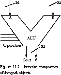
The 32-bit A and B data inputs come from other sources in the data-path; the S output goes to a data-path destination. The operation signals come from the control unit; the carry-out signal is routed back to the control unit so that it may detect certain exceptional conditions, such as overflow, that may disrupt the normal sequencing of instructions. We construct other data-path objects, such as shifters, registers, and register files, in an analogous manner.
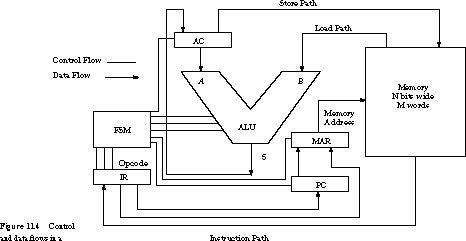
Figure 11.4 shows the block diagram for such a single accumulator machine.
Instructions for a single accumulator machine are called
single address instructions. This is because they contain only
a single reference to memory. One operand is implicitly the AC; the other
is an operand in memory. The instructions are of the form AC :=
AC <operation> Memory (Address). <operation>
could be ADD, SUBTRACT, AND, OR, and so on.
Let's consider an ADD instruction. The old value of the
AC is replaced with the sum of the AC's contents and the contents of the
specified memory location.
Data and Control Flows Figure 11.4
shows the flow of data and control between memory, the control registers
(IR, MAR, and PC), the data re-gister (AC),
and the functional units (ALU). The MAR is the
Memory Address Register, a storage element that holds the address
during memory accesses. Data flows are shown as bold arrowed lines; the
other lines represent control.
The core of the data-path consists of the arithmetic logic
unit and the AC. The AC is the source or destination of all transfers. These
transfers are initiated by store, arithmetic, or load operations. Let's
look at them in more detail.
The instruction identifies not only the operation to be
performed but also the address of the memory operand. Store operations move
the -contents of the AC to a memory location specified by bits within the
instruction. The sequencing begins by moving the specified address from
the IR to the MAR. Then the contents of the AC are placed on the memory's
data input lines while the MAR is placed onto its address lines. Finally,
the memory control signals are cycled through a write sequence.
Arithmetic operations take as operands the contents of
the accumulator and the memory location specified in the instruction. Again,
the control moves the operand address from the IR to the MAR, but this time
it invokes a memory read cycle. Data obtained from the load path is combined
with the current contents of the AC to form the operation result. The result
is then written back to the accumulator.
A load operation is actually a degenerate case of a normal
arithmetic operation. The control obtains the B operand along the
load path from memory, it places the ALU in a pass-through mode, and it
stores the result in the AC.
Whereas load/store and arithmetic instructions manipulate
the AC, branch instructions use the PC. If the instruction is an unconditional
branch, the address portion of the IR replaces the PC, changing the next
instruction to be executed. Similarly, a conditional branch replaces the
PC if a condition specified in the instruction evaluates to true.
Placement of Instructions and Data There
are two possible ways to connect the memory system to the CPU. The first
is the so-called Princeton architecture: instructions and data
are mixed in the same memory. In this case, the instruction and load/store
paths are the same.
The alternative is the Harvard architecture.
Data and instructions are stored in separate memories with independent paths
into the processor.
The Princeton architecture is conceptually simpler and
requires less connections to the memory, but the Harvard architecture has
certain performance advantages. A Harvard architecture can fetch the next
instruction even while executing the current instruction. If the current
instruction needs to access memory to obtain an operand, the next instruction
can still be moved into the processor. This strategy is called instruction
prefetching, because the instruction is obtained before it is really
needed. A Princeton architecture can prefetch instructions too. It is just
more complicated to do so. To keep the discussion simple, we will assume
a straightforward Prince-ton architecture in the rest of this chapter.
Detailed Instruction Trace As an
example of the control signal and data flows needed to implement an instruction,
let's trace a simple instruction that adds the contents of a specified memory
location to the AC:
We write the operation statements in terms of the control
signals to be asserted, such as Memory Read, ALU ADD, or PC
increment. We write register-to-register transfers in the form source
register Æ destination register. The detailed pathways
between registers determine the more refined register transfer description.
We will see more register transfer descriptions in Section 11.2.
The key elements are the two special registers, MAR and MBR, and the
three control signals, Request, Read/![]() , and Wait. Let's
start with the registers.
, and Wait. Let's
start with the registers.
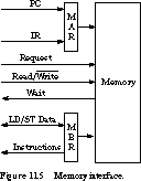
We have seen the MAR before. In Figure 11.5, it can
be loaded from the program counter for instruction fetch or from the IR
with a load or store address. To decouple the memory from the internal working
of the processor, we introduce a second interface register, the Memory
Buffer Register, or MBR. A bidirectional path for load/store data exists
between the processor data-path and the MBR, while the pathway for instructions
between the MBR and IR is unidirectional.
Besides the address and data lines, the interface to memory
consists of three control signals. The Request signal notifies the memory
that the processor wishes to access it. The Read/![]() signal specifies
the direction: read from memory on a load and write to memory on a store.
The Wait signal lets memory stall the processor, in effect, notifying the
processor that its memory request has not yet been serviced. We can think
of Wait as the complement of an acknowledgment signal.
signal specifies
the direction: read from memory on a load and write to memory on a store.
The Wait signal lets memory stall the processor, in effect, notifying the
processor that its memory request has not yet been serviced. We can think
of Wait as the complement of an acknowledgment signal.
Processor-Memory Handshaking In
their most general form, the memory system and the processor do not share
a common clock. To ensure proper transfer of data, we should follow the
four-cycle signaling convention of Section 6.5.2. The processor asserts
the read/write direction, places data in the MAR (and the MBR
if a write), and asserts Request. The memory normally asserts
Wait, unasserting it when the read or write is complete.
When the processor notices that Wait is no longer asserted,
it latches data into the MBR on a read or tri-states the data connection
to memory on a write. The processor unasserts its Request line and must
wait for the Wait signal to be reasserted by the Memory before it can issue
its next memory request.
The signaling waveforms are shown in Figure 11.6.
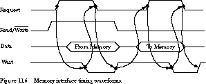
The four-cycle handshake of the Request and Wait signals for the read sequence work as follows:
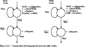
Figure 11.7 shows possible state machine fragments for implementing the
four-cycle handshake with memory. We assume a Moore machine controller implementation.
In the read cycle, we enter a state that drives the address bus from the
MAR, asserts the Read and Request signals, and latches the data bus into
the MBR. This last transfer catches correct data only if memory has unasserted
Wait, so we must loop in this state until this is true. On exit to the next
state, the Request signal is unasserted and the address bus is no longer
driven. The memory signals that it is ready for a new request by asserting
Wait. To remain interlocked with memory, we loop in this state until Wait
is asserted. The write cycle is similar.
Depending on detailed setup and hold time requirements,
it may be necessary to insert additional states in the fragments of Figure
11.7. For example, if the memory system requires that the address lines
and read/write direction be stable before the request is asserted, this
should be done in a state preceding the one that asserts Request.
Remember that only the register transfer operations being
asserted in a given state need to be written there. If an operation is not
mentioned in a state (or state transition for a Mealy machine),
it is implicitly unasserted. Thus, you don't have to explicitly set Request
to its unasserted value in the second state of the handshake fragments.
However, you should include such register transfer operations to improve
the clarity of your state diagram.
I/O access times are measured in milliseconds, whereas
memory access times are usually less than a microsecond. It isn't productive
to hold up the processor for thousands of instruction times while the I/O
device does it job. Therefore, the control coupling between the processor
and I/O devices is somewhat more complex than the memory interface.
Polling Versus Interrupts Because
of the (relatively) long time to execute I/O operations,
they are normally performed in parallel with CPU -processing. An I/O device
often has its own controllers, essentially an in-de-pen-dent computer that
handles the details of device control. The CPU asks the controller to perform
an I/O operation, usually by writing in-for-ma-tion to memory-mapped control
registers. The processor continues to exe-cute a stream of instructions
while the I/O controller services its request.
The I/O controller notifies the CPU when its operation
is complete. It can do this in two main ways: polling and interrupts.
In polling, the I/O controller places its status in a memory-mapped register
that the CPU can access. Every once in a while, the system software running
on the CPU issues an instruction to examine the status register to see if
the request is complete.
With interrupts, when the I/O operation is complete, the
controller asserts a special control input to the CPU called the interrupt
line. This forces the processor's state machine into a special interrupt
state. The current state of the processor's registers, such as the PC and
AC, is saved to special memory locations. The PC is overwritten with a distinguished
address, where the system software's code for interrupt handling can be
found. The instructions at this location handle the interrupt by copying
data from the I/O device to memory where other programs can access it.
Polling is used in some very high performance computers
that cannot afford to have their instruction sequencing disturbed by an
I/O device's demand for attention. Interrupt-based I/O is used in almost
all other computers, such as personal computers and time-sharing systems.
Changes to the Control State Diagram We
need only modest changes to add interrupt support to the basic processor
state diagram of Figure 11.2. Before fetching a new instruction, the processor
checks to see whether an interrupt request is pending. If not, it continues
with normal instruction fetch and execution.
If an interrupt has been requested, the processor simply
enters its special interrupt state sequence. It saves the state of the machine,
particularly the PC, and tells the I/O device through a standard handshake
that it has seen the interrupt request. At this point, the machine returns
to normal instruction fetch and execution, except that the PC now points
to the first instruction of the system software's interrupt handler code.
A machine with interrupts usually provides a Return from
Interrupt instruction. The system software executes this instruction at
the end of its interrupt handling code, restoring the machine's saved state
and returning control to the program that was running when the interrupt
took place.
[Top] [Next]
[Prev]