Lab 4
Test Equipment
Lab 4
Building buggy hardware is easy, so you need some way to debug it.
Hwdebugger is a fantastic tool for debugging your xilinx hardware, but it has its limits.
This lab will familiarize you with more hardware debugging tools.
Each station in 204B has a triple-output bench power supply, a digital
multimeter, a pulse generator, and a 100 MHz mixed signal oscilloscope. You will use each of these in this lab.
Test equipment can be complex. The oscilloscope has more than forty
knobs and switches. Unfortunately, missetting these can make the
equipment appear broken.
If you suspect faulty equipment, verify it with your TA!
When you leave the lab, please tidy up around your station.
As usual, read through this lab. Most of this handout describes
things to know, not things to do. And these should be easy if you
know how to do them.
Each station has an HP E3630A triple-output power supply, whose three
outputs can generate 0-6V, 0-20V, and -20-0V, marked +6, +20 and -20 respectively. There is also a ground connection labeled
COM.
The HP's outputs are current-limited for safety: they will supply some
maximum amount of current, and will drop the output voltage to ensure
it. In particular, if you short the outputs, instead of blowing fuses
or becoming arc welders, these supplies peacefully supply the maximum
current.
The HP's three knobs set the voltage on the +6 output, the voltage
on the +20 output, and the ratio between the +20 and -20
outputs. Turn clockwise (to FIXED) until clicks to set ratio to 1.
The HP's analog meter can display the voltage of each output, selected
with the three buttons
labeled +6, +18, and -18. This is useful for setting the
voltages approximately, but it is not as accurate as measuring the
output voltage with a digital multimeter.
Each station also has a Fluke 8010A digital multimeter, which can
measure AC or DC voltage, current, resistance, or conductivity.
- Measuring Voltage
Press button marked V and select range with one of the grey buttons. Connect the COMMON input (a black lead) to the circuit's
ground, and connect the V/k /S input (a red lead) to the
voltage to measure.
/S input (a red lead) to the
voltage to measure.
- Measuring Current
Press button marked mA. Connect the COMMON input and either the mA or the 10A max
input in series with the wire whose current you wish to measure.
This requires disconnecting the wire, often after the circuit is
powered down.
- Measuring Resistance or Conductance
Press button marked k/S. With the circuit power off, connect the COMMON (black) and
V/k/S (red) leads across the resistive element. To do this
accurately, the element usually has to be removed from the circuit,
although simple continuity checking (determining if a wire is
connected) can be done in-circuit.
The pulse generator can generate single or periodic square waveforms
with varying voltages, periods, duty cycles, pulse widths, and slew
rates. These can be used, for example, as a digital system's clock.
The output of the pulse generator has a  output impedance,
and expects to be driving a load. Thus, with
high-impedance inputs such as those on digital logic or a scope, the
voltage you observe will be twice as large as what you set.
output impedance,
and expects to be driving a load. Thus, with
high-impedance inputs such as those on digital logic or a scope, the
voltage you observe will be twice as large as what you set.
To produce a square wave,
-
Make sure the DISABLE button (in the lower right corner) is
off (unlit).
-
Set MODE to NORM by pressing the button beneath it. (second to left)
-
Set CTRL to disabled (nothing lit). (fourth to left)
-
Press the button underneath PER until the PER lights, and set the
period using the vernier buttons.
-
Press the button underneath DTY until the DTY lights, and set the duty
cycle using the vernier buttons.
Or, set the pulse width ( ) by
pressing the same button until WID lights. Adjust using the vernier
buttons.
) by
pressing the same button until WID lights. Adjust using the vernier
buttons.
-
Press the button under HIL and set the high voltage using the
vernier buttons.
-
Press the button under LOL and set the low voltage using the
vernier buttons.
Oscilloscopes can display very high-speed periodic events. Think of
them as things that graph voltage versus time.
Figure 1 shows an oscilloscope's major component: the
cathode ray tube (CRT), similar to that in a television. A large
voltage (our scope uses 14,000 V) is placed across anode and cathode,
causing electrons to fly from the negatively-charged cathode, through
a vacuum, and smash into the positively-charged anode, illuminating a
spot on its phosphorus coating. This bright spot disappears quickly,
so for an image to appear stable, it must be redrawn many times a
second.
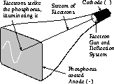
Figure 1: An Oscilloscope's Cathode Ray Tube (CRT)
To display a repeating waveform, the oscilloscope periodically
''sweeps'' the beam from left to right, vertically deflecting the beam
proportional to the input voltage. The result is a graph with time
increasing to the right, voltage increasing up: like a timing diagram.
Starting the sweep at the right time is necessary for a stable image.
Figure 2a shows the effect of choosing the wrong
times: many segments of the waveform are superimposed, resulting in an
unreadable mess. If these times are chosen correctly, i.e., at some
exact multiple of the period of the waveform, the traces superimpose
to give a single, stable waveform, as shown in
Figure 2b.
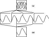
Figure 2: (a) Incorrect triggering. (b) Correct triggering.
Most oscilloscopes allow the user to set a voltage and a slope (rising
or falling) for the trigger. For example, in
Figure 2b, the trigger is the voltage halfway between
the two extremes, with a falling slope. For simple waveforms, this by
itself works well. For more complex waveforms, the variable holdoff
control can help, which sets the time between the end of a sweep and
when the scope starts looking for the trigger.
Not everything interesting is periodic; fortunately some oscilloscopes
can record a single event and display it indefinitely. Once, such
storage scopes used a clever electrical trick to keep the phosphors
illuminated, but the advent of cheap, fast digital logic and memory
made these obsolete.
DSOs, or digital storage oscilloscopes, digitize their inputs, store
them in memory, and recall them through a digital-to-analog converter.
Using a storage scope is much like using a non-storage scope: set the
trigger to catch what you want and view the results. Instead of
displaying the waveform for each trigger, however, a storage scope can
await a single trigger, capture the waveform, and display it until you
store another.
Although four-channel scopes exist, most digital circuits have far
more than four interesting signals, and the ``interesting'' things on
those signals are too complex for an oscilloscope's simple trigger to
find. Logic analyzers address these problems.
Logic analyzers are like many-channeled storage oscilloscopes with
very sophisticated schemes for triggering. Some logic analyzers have
hundreds of channels, and the triggers can be little programs
consisting of comparisons, loops, and branches. Logic analyzers
capture and store digital waveforms only (i.e., usually only two
voltage levels), and are typically not as fast as oscilloscopes. But
for finding subtle, aperiodic bugs in digital hardware, they are
unmatched.
The HP 54645D is both a Digital Storage Oscilloscpe and a simple Logic Analyzer
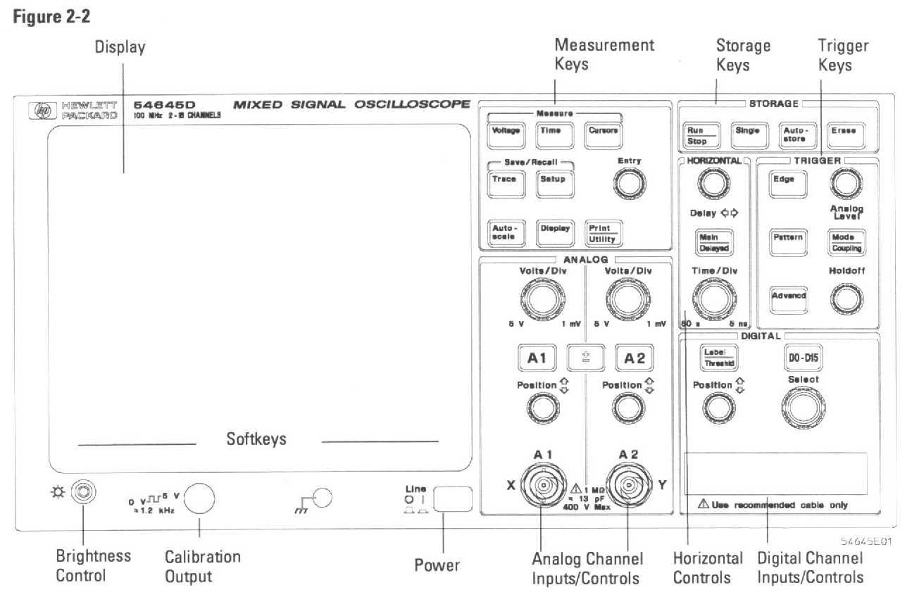
Figure 3: Groups of controls on
the 54645D
The 54645D has some forty knobs, buttons, and switches. Even for this
lab, you need to know most of them. Fortunately, using one
oscilloscope is like using another, so learning one is worth your
time.
Here is a list of controls that concern you for this lab, grouped as
in Figure 3:
SOFTKEYS
-
-
The functions for these keys are displayed on the screen of each particular mode of operation
-
-
Brightness control adjusts the intensity of the display.
- If nothing appears on the screen, try adjusting the brightness control
Calibration Output
-
This hook is used to test probes. Whenever in doubt, attach probe to calibration output and hit AUTO-SCALE button in measurement section. It should display a nice 0-5V square wave at about 1.232kHz
AUTOSCALE
- This button is located in the measurement section. Perhaps most frequently used button. Scope automatically searches for a signal, sets time and voltage ranges to place signal in middle of screen.
IF SIGNAL DISAPPEARS, TRY HITTING AUTOSCALE
MEASUREMENT CONTROLS
- Consists of three buttons; VOLTAGE, TIME, and CURSORS. VOLTAGE and TIME will place options on types of measurements (Vave, Vp-p, Freq, ect.) above softkeys. When selected, measurement will be displayed at bottom of screen. The SOURCE softkey should be set on correct analog source channel. The CURSORS button is used to display or clear time and voltage measurement cursors which are selected with softkey and moved with ENTRY knob.
SAVE/RECALL
-
TRACE
- Allows you to store waveforms in two memories. Signals saved and recalled with softkeys.
SETUP
- Allows you to undo autoscaling, recover screens, and setup display defaults.
DISPLAY AND PRINT UTILITY
- Softkeys set display and grid lines.
Make sure mode is set to normal with vectors on.
ANALOG
- VOLT/DIV
- Increase gain at which signal is observed. Volts per grid block is given at top of screen.
A1, A2, and +-
- A1 and A2 allow you to turn on and off each channel. High or low pass filtering with softkeys, AC or DC couplingcan be used to get rid of excess noise. But note: Noise reduction decreases trigger sensativity.
+- allows you to do sums and differences of signals.
HORIZONTAL
- DELAY knob moves time reference left or right.
Main Delayed
Horizontal mode should be set at normal with softkeys, the TIME REF softkey controls what reference to use when zooming in with TIME/DIV knob. VERNIER is used to minimize time steps in TIME/DIV knob.
TIME/DIV
- Changes time per grid block in a 1-2-5 fashion. Values are displayed at the top of the screen. Try setting this to the smallest setting (~2ns) and zoom in on a signal. Hit the RUN/STOP button to freeze the screen and witness the degradation of smoothness in the signal. Can you explain this?
DIGITAL
-
Label/Threshold
-
Allows you to label one of the 16 probe leads of the logic analyzer. The threshold menu and softkeys let you choose what type of logic. CMOS or TTL should work fine.
D0-D15
- This button allows you to select which logic analyzer probes will be displayed. Signals can be selected with SELECT knob and turned on or off with softkeys
Position- Lets you reorder signals
TRIGGER
- Edge
- Lets you pick trigger source and select rising or falling edges.
Pattern- Allows you to trigger on a pattern of signals. Used with SELECT in "digital" region and softkeys.
Analog level & Holdoff
- Lets you select voltage level to trigger at. It should be used with analog signals. Holdoff controls amount of time to wait before new screen is drawn. Should be set to minimum value
STORAGE
- RUN/STOP
- Starts and stops refresh on display and can be used with TRIGGER to start automatically. TIME/DIV also determines how much signal will be stored on screen.
SINGLE- Takes a single frame rather than looping like RUN.
AUTOSTORE- Will superimpose previous traces.
ERASE
- Erases stored or stooped signals, measurements should be restarted with RUN button.
TIPS ON TRIGGERING FOR THE LAB
- To trigger off a signal edge:
- Hit EDGE
Select a channel as the trigger source using either the SELECT knob or by pressing a Trigger Source softkey.
Press one of the Edge softkeys to choose whether the trigger will occur on the rising or falling edge.
To define a pattern trigger-
Press PATTERN
Rotate the SELECT knob through each signal (D0-D15) and (A1 or A2), which is displayed above the Source softkey.
Then, press one of the softkeys to set the condition the oscilloscope will recognize as part of the pattern for that channel:
- L for logic low
H for logic high
X to ignore this channel
Rising or falling edge
_______________________________________________________________
-
Use banana leads to connect the output of the power supply to the
input of the multimeter. Use black for common, red for power.
-
Adjust the supply to simultaneously generate  V,
V,  V, and
 V, and measure this with the multimeter. Show your TA this.
-
Connect the output of the HP 8112A Pulse Generator to Channel 1 of
the scope using a coaxial cable with BNC ends.
-
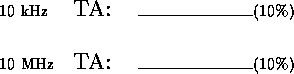
Set the pulse generator to generate a 10 kHz, 45% duty cycle, 4
volt peak-to-peak, zero volt offset (i.e., peaks at  V) square
wave.
V) square
wave.
-
Display this square wave using the STORE
mode of the scope. In the STORE mode, use the cursors to
verify the pulse width, frequency, and voltages. Show your TA this.
-
Set the pulse generator to generate a 10 MHz, 0-5V square wave with
a 40 ns pulse width.
-
Again, store the display, and verify the pulse width, frequency and voltages. Show your TA this.
We have entered and compiled the circuit in Figure 4, a
four-bit counter driving the addresses of three sixteen-bit ROMs.
Your task will be to use both channels of the oscilloscope to observe
the outputs of ROM2 and ROM3 and deduce their contents, using the
contents of ROM1 as a starting point.
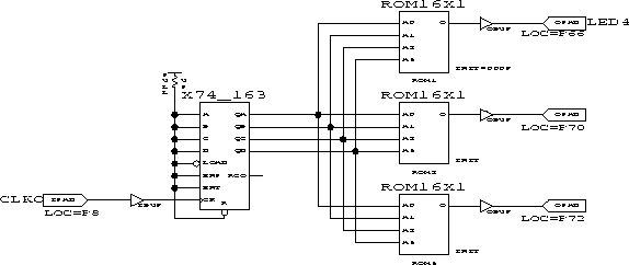
Figure 4: Three ROMs
The counter counts 0000, 0001, ..., 1111, and
repeats.. Address 0000 reads the least significant bit of the
four-digit hex number in the ROM, address 1111 the most. So if
one of the ROMs contained a zero in address 0000 and ones in addresses 0001 through 1111, the ROM contents would be
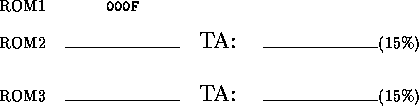
FFFE. See the ROM16X1 page in your reader for more information.
-
Fire up Hwdebugr and load the ROM circuit- U:/WVLIB/CS150/ROM.BIT. Open the Control Panel from the View menu and start the clock. If all goes well, the fourth LED will light (the output of ROM1).
-
Connect the BNC ends of the scope probes to the scope's
Channel 1 and Channel 2 inputs. These are  probes, so the
volts/div reading on the scope's display will be a tenth of the
circuit's voltages.
probes, so the
volts/div reading on the scope's display will be a tenth of the
circuit's voltages.
-
Carefully connect each probe's ''hook'' to one of the wire-wrap pins
connected to a Xilinx pin connected to a ROM's output. Be
careful not to short together two pins, and don't let the probe bend
the pin. Connect Channel 1 of the oscilloscope to the output of ROM1, whose contents
you know (Figure 4), and connect Channel 2 to the output of one of the others.
-
Connect both probes' alligator clips to a ground reference in
the prototyping area of the board.
-
Set the oscilloscope to trigger on Channel 1 (the output of ROM1),
and display both channels.
-
Turn on the vernier mode on the oscilloscope (MAIN/DELAYED), and then adjust the TIME/DIV knob so that there is exactly two bits per division-adjust it so eight
divisions occur between rising edges in the output of ROM1.
-
Read off the bits from each ROM, moving the Channel 2 probe between
pins to view the contents of the two ROMs, and translate each into a
four-digit hex number. Record these on the checkoff sheet and show
your TA.
We have entered and compiled the circuit in Figure 5, a
eight-bit ripple adder summing the output of a four-bit counter and
four switches. Your task will be to measure the worst-case delay of
the circuit.
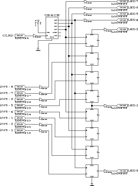
Figure 5: An eight-bit adder
The worst-case delay occurs when a carry must ripple through each
stage, such as when 1111 and 0001 are added. To find
this, set the switches to 0001, and set the logic analyzer (Probes on DIGITAL section) to
trigger when the counter hits 1111.
-
Fire up Hwdebugr and load the adder- U:/WVLIB/CS150/ADD.BIT.
Since the outputs all go to LEDs, this circuit is an excellent one
to single-step with the clock. From the Readback Control Panel, set the clock steps to 1 and use APPLY to step the counter. The adder will still work even
when the clock is stopped. Remember that the LEDs light when their
output is low.
-
Connect the logic analyzer's pod's black ground lead to a ground
reference (e.g., one of the ground pins on the Xilinx), and connect
seven of the eight inputs to the four counter outputs and three
adder outputs.
Be careful when connecting the probe leads. They are delicate
and expensive, even more so than the wire-wrap posts.
-
Set the switches so 00000001 is one of the addends. (See Figure. 5 to determine which switch should be least significant)
-
Set the trigger on the logic analyzer to when the counter reaches
1111.
-
Measure the delay from when the counter output changes to when the
final carry-out changes, and record this on the checkoff sheet.
Show your TA this.
Names:
- __________________
__________________
Lab Section:__________________
-
Power Supply and Multimeter
TA:
(10%)
-
Pulse Generator and Oscilloscope
-
ROMs
-
Logic Analyzer Delay:
TA:
(30%)
-
Done Early (During Lab):
TA:
(10%)
polkeem@cory.berkeley.edu